14 Layer High Thickness Diameter Ratio Semiconductor Test Thick
Gold Plate
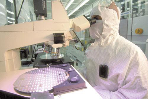
The 14 layer high thickness diameter ratio semiconductor test thick
gold board is a semiconductor test high-rise PCB circuit board
developed and produced by Shenzhen Quanhong Electronics Co., Ltd.
It is made of Shengyi s1000-2m material and thick gold plating on
the surface. The minimum line width and line distance can reach 100
/ 90um, and the minimum mechanical hole can reach 0.35mm. It is
mainly used in the field of semiconductor testing and is an ideal
choice in the field of semiconductor testing.
HLC Process capability
| Item | HLC Advanced Technology |
| 2019 | 2020 | 2021 |
| Max Panel Width (inch) | 25 | 25 | 25 |
| Max Panel Length (inch) | 29 | 29 | 29 |
| Max Layer Count (L) | 16 | 18 | 36 |
| Max Board thickness (mm) | 3.2 | 4 | 6 |
| Max Board thickness Tolerance | +/-10% | +/-10% | +/-10% |
| Base copper Thickness | Inner layer ( OZ ) | 4 | 6 | 8 |
| Outer Layer ( OZ ) | 2 | 3 | 4 |
| Min DHS ( mm ) | 0.2 | 0.15 | 0.15 |
| PTH Size Tolerance ( mil ) | +/-2 | +/-2 | +/-2 |
| Back Drill (stub)( mil ) | ~ 3 | ~ 2.4 | ~ 2 |
| Max. AR | 12:1 | 16:1 | 20:1 |
| Item | HLC Advanced Technology |
| 2019 | 2020 | 2021 |
| M-drill tolerance | Inner layer ( mil ) | DHS + 10 | DHS + 10 | DHS + 8 |
| Outer Layer ( mil ) | DHS + 8 | DHS + 8 | DHS + 6 |
| Solder mask Registration (um) | +/- 40 | +/- 30 | +/- 25 |
| Impedance control | ≥50ohms | +/-10% | +/-10% | -/-8% |
| <50ohms | 5 Ω | 5 Ω | 4 Ω |
| Min LW/S (Inner)@1oz base Cu ( mil ) | 3.0 / 3.0 | 2.6 / 2.6 | 2.5 / 2.5 |
| Min LW/S (Outer)@1oz Cu ( mil ) | 3.5 / 3.5 | 3.0 / 3.5 | 3.0 / 3.0 |
| Max dimple for POFV ( um ) | 30 | 20 | 15 |
| Surface Finishing | ENIG, Immersion Ag, OSP, HASL, Immersion Tin, Hard Au |
HDI Process capability
| Item | HDI Advanced Technology |
| 2019 | 2020 | 2021 |
| Structure | 5+n+5 | 6+n+6 | 7+n+7 |
| HDI Stack Via | AnyLayer(12L) | AnyLayer(14L) | AnyLayer(16L) |
| Board Thickness(mm) | Min. 8L | 0.45 | 0.4 | 0.35 |
| Min. 10L | 0.55 | 0.45 | 0.4 |
| Min. 12L | 0.65 | 0.6 | 0.55 |
| MAX. | | 2.4 | |
| Min. Core Thickness ( um ) | 50 | 40 | 40 |
| Min. PP Thickness ( um ) | 30(#1027PP) | 25(#1017PP) | 20(#1010PP) |
| Base Copper Thickness | Inner Layer ( OZ) | 1/3 ~ 2 | 1/3 ~ 2 | 1/3 ~ 2 |
| Outer Layer ( OZ ) | 1/3 ~ 1 | 1/3 ~ 1 | 1/3 ~ 1 |
| Item | HDI Advanced Technology |
| 2019 | 2020 | 2021 |
| Min. Mechanical Drill hole size(um) ** | 200 | 200 | 150 |
| Max. Through Hole Aspect Ratio * | 8:1 | 10:1 | 10:1 |
| Min. Laser via/Pad Size ( um ) | 75/200 | 70/170 | 60/150 |
| Max. Laser Via Aspect Ratio | 0.8:1 | 0.8:1 | 0.8:1 |
| Laser Via on PTH(VOP)design | Yes | Yes | Yes |
| Laser X type through hole(DT≤200um) | NA | 60~100um | 60~100um |
| Min. LW/S (L/S/Cu, um) | Inner Layer | 45 /45 /15 | 40/ 40/ 15 | 30/ 30 /15 |
| outer Layer | 50 /50/ 20 | 40 /50 /20 | 40 /40 /17 |
| Min BGA Pitch (mm) | | 0.35 | 0.3 | 0.3 |
| Item | HDI Advanced Technology |
| 2019 | 2020 | 2021 |
| Solder mask Registration (um) | +/- 30 | +/- 25 | +/- 20 |
| Min. Solder Mask Dam (mm) | 0.07 | 0.06 | 0.05 |
| PCB Warpage Control | >= 50ohm | +/-10% | +/-8% | +/- 5% |
| < 50ohm | +/- 5ohm | +/- 3ohm | +/- 3ohm |
| PCB Warpage Control | ≤0.5% | ≤0.5% | ≤0.5% |
| cavity Depth accuracy (um) | Mechanical | +/- 75 | +/- 75 | +/- 50 |
| Laser directly | +/- 50 | +/- 50 | +/- 50 |
| Surface Finishing | OSP,ENIG,Immersion Tin,Hard Au, Immersion Ag | OSP,ENIG,Immersion Tin,Hard Au,Immersion Ag, ENEPIG |
| Packaging & Delivery |
| Packaging Details: | Inner: vacuum packing or Anti-static package,
Outer: export carton
or according to the customer's requirement. |
| Port: | Shenzhen or Hongkong |
| Lead Time: | Quantity(Pieces) | 1-10 | 11-100 | 101-1000 | >1000 |
| Est. Time(days) | 3-5 | 3-5 | 7-9 | To be negotiated |
FAQ:
Q: What service do you have?
FASTPCB: We provide turnkey solution including PCB fabrication,
SMT, plastic injection & metal,final assembly, testing and other
value-added service.
Q: What is needed for PCB & PCBA quotation?
FASTPCB: For PCB: Quantity, Gerber file and technic
requirements(material,size, surface finish treatment, copper
thickness,board thickness).
For PCB: PCB information, BOM,Testing documents.
Q: How to keep our product information and design file secret ?
FASTPCB: We are willing to sign a NDA effect by customers side
local law and promising tokeep customers data in high confidential
level.
Q: What are the main products of your PCB/PCBA services?
FASTPCB: Automotive, Medical, Industry Control, IOT, Smart Home,
Military, Aerospace.
Q: What is your minimum order quantity (MOQ)?
FASTPCB: Our MOQ is 1 PCS, sample and mass production all can
support.
Q: Are you factory?
FASTPCB:Shangxing West Industrial Zone, Xihuan Road, Shajing
Street, Bao 'an District, Shenzhen, Guangdong province, China